|
Input files
|
LoopOnSurface.MIN, LoopOnSurface.PIN, LoopOnLayerScan.BAT, LoopOnLayerScan.MIN, LoopOnLayerScan.PIN, LoopOnLayerScan.SCR, LoopOnLayerThick.png, LoopOnLayerThin.png
CurrentLoopYIG
|
|
Description
|
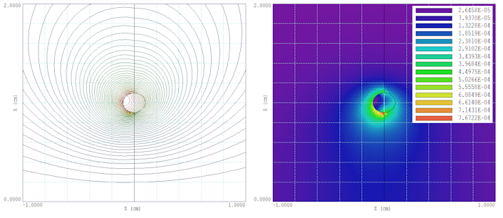
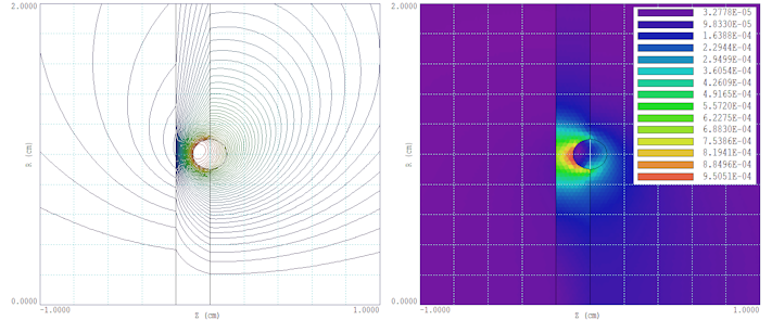
Recently, we received an inquiry about the magnetic field distribution created by a microscopic current loop deposited on a YIG film. Although the geometry is simple, the results are interesting and somewhat unexpected. The loop in the application had a diameter of about 2 um with a conductor radius of about 0.2 um. For generality, we set up a solution with a loop diameter D = 2.0 cm and a wire diameter d = 0.2 cm. The loop carries current I = 1.0 A. Scaling can be applied for applications in different size ranges. The top figure shows the geometry near the loop in an r-z plot (note: in such a plot, only positive values of r are defined). The solution boundaries are much larger to minimize their effect. The region to the left of center can be assigned as air, YIG (with MuR = 15.0) or a YIG film (as in the lower figure). It is assumed the material is unsaturated at practical current levels.
|
|
Results
|
In an initial run, the left-hand region was taken as air (MuR = 1.0). The predicted inductance is given by:
L ~ Mu0*MuR*(D/2)*[ln(8*D/d)-2]
The value for the calculation parameters is 29.94 nH. The code value (equal to 2*U, where U is the total field energy minus that in the wire) is 29.55 nH. The 1.3% difference results from the finite solution volume. The calculated field at the center (Bz(0,0) = 6.251E-5 T) is close to the theoretical value
Bz(0,0) = Mu0*I/D = 6.283E-5 T.
With a uniform relative magnetic permeability of 15.0 set over the full solution volume, the calculated inductance is L = 440.0 nH, a factor of 14.9 higher. The difference represents the contribution of the wire at MuR = 1.0.
The top figure shows the field lines and |B| distribution with MuR = 15.0 on the left and MuR = 1.0 on the right. The field lines are almost identical to the vacuum case with a small shift into the ferrite. The inductance is 56.52 nH. Both the inductance and field values are about a factor of 1.9 higher than the air calculation. The reason is that the reluctance is dominated by the air region. The presence of the ferrite reduces it by only a factor of about 2.
The field line pattern in the top figure differs only slightly from the vacuum solution. The lower figure shows the field distribution for YIG layer thin compared to the wire diameter, Delta = 0.2 cm = 0.1D. The table list the results of a calculation of inductance a function of the layer width. The conclusion is the inductance enhancement has only a weak dependence of the YIG layer thickness.
   Delta/D        Delta           U              L
  =====================================================
     Inf           Inf        2.826E-8       5.652E-8
     1.00          2.0        2.823E-8       5.646E-8
     0.50          1.0        2.810E-8       5.620E-8
     0.25          0.5        2.758E-8       5.516E-8
     0.10          0.2        2.557E-8       5.114E-8
|
|
Comments
|
The results can be scaled to microscopic dimensions. Suppose we make the transformation D: 2.0 => 2E-4 cm, d: 0.2 => 0.2E-4 cm, I: 1.0 A => 50 mA. The inductance is reduced by a factor of 10,000 and the field level is increased by a factor (10,000)(0.05) = 500. The field at the loop center for the microscopic system is about 30 G.
|